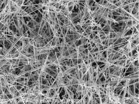
Specification of Copper Nanowires:
Diameter:50-200nm
Length:1-10um
Purity:99%
Note: We can supply different size products of Copper Nanowires according to client's requirements.
Copper nanowires in metal nanowires can meet the material requirements of future optoelectronic devices due to their good electrical, mechanical and chemical properties. At the same time, the low price and abundant storage of copper nanowires make the research on copper nanowires equally important, so it is regarded as one of the most promising flexible transparent electrode materials. In addition, due to the large aspect ratio effect of copper nanowires, it also has outstanding advantages in the application of conductive adhesives and thermal conductive adhesives. Transparent conductive materials that are expected to replace ITO are doped with ZnO, carbon nanotubes, graphene, metal gates, and metal nanowires.
Application of Copper Nanowires:
1. Application in catalysis
Copper nanowires have excellent catalytic activity and reaction selectivity, which can improve the reaction efficiency. Because of their catalytic activity selectivity, they are much higher than traditional catalysts and are used as catalysts for various reactions.
2. Applications in the field of optics
Copper nanowires have excellent photoelectric effect, and due to the ultra-fast nonlinear optical response near the surface plasmon oscillation absorption peak, the composite materials prepared by doping copper nanowires in semiconductors or insulators can obtain higher photoexcitation. Rate and extremely strong third-order nonlinear polarizability coefficients. These optical properties make copper nanowires widely used in the field of optics.
3. Application in the field of electrodes
The copper nanowire has excellent electrical conductivity, and also has excellent light transmittance, flexural resistance, and low production cost. And copper nanowires are entirely possible to achieve large-area material preparation through the spraying process, and are regarded as one of the most potential flexible transparent electrode materials.
4. Applications in other fields
Due to the large aspect ratio effect of copper nanowires, the ultra-high electrical and thermal conductivity also has outstanding advantages in the application of conductive paste, conductive adhesive, thermal conductive adhesive and the like.
SEM of Copper Nanowires:
Storage conditions:
Copper Nanowires should be sealed and stored in a dry and cool environment. It should not be exposed to the air for a long time, to prevent agglomeration due to moisture, affecting the dispersion performance and use effect, and should avoid heavy pressure, do not contact with oxidant, and transport according to ordinary goods.

