Blind
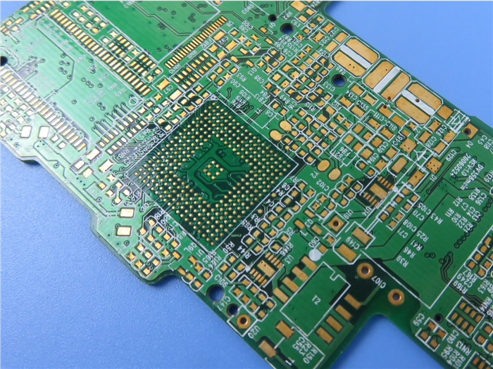
Via PCB Built on Tg150℃ FR-4 With Immersion Gold 4-Layer FR-4 Circuit Board
(Printed
circuits boards are custom-made products, the picture and parameters shown are
just for reference)
1.1
General description:
It's 1.6 mm thick with
white silkscreen(Taiyo) on green solder mask (Taiyo) and immersion gold on
pads. The base material is from ITEQ supplying single up PCB. They're
fabricated per IPC 6012 Class 2 using supplied Gerber data. Each 25 boards are
packed for shipment.
1.2
Features and Benefits :
1.2.1
Middle Tg FR-4 Shows low Z-CTE and excellent through hole reliability;
1.2.2 Immersion
gold has high solderability, no stressing and less contamination;
1.2.3
Multilayer shortened connection between electronic components;
1.2.4
16000㎡workshop and 8000 types of
PCB's per month;
1.2.5
Delivery on time: >98%
1.2.6
No minimum order quantity. 1 piece is available;

1.3
Applications:
Industrial
Computer
GPS
Tracking System
POS
Cash Register
Embedded
Systems
Data
Acquisition System
Microcontrollers
PC
and Notebook
1.4
Parameter and data sheet:
|
PCB SIZE
|
119 x 80mm=1PCS
|
|
BOARD TYPE
|
Multilayer
PCB
|
|
Number
of Layers
|
4 layers
|
|
Surface
Mount Components
|
YES
|
|
Through
Hole Components
|
YES
|
|
LAYER STACKUP
|
copper
------- 18um(0.5oz)+plate TOP layer
|
|
Core FR-4 0.61mm
|
|
copper ------- 35um(1oz) MidLayer 1
|
|
Prepreg 0.254mm
|
|
copper ------- 35um(1oz) MidLayer 2
|
|
Core FR-4 0.61mm
|
|
copper -------
18um(0.5oz)+plate BOT layer
|
|
TECHNOLOGY
|
|
|
Minimum Trace and Space:
|
4
mil / 4 mil
|
|
Minimum
/ Maximum Holes:
|
0.3
mm /3.5 mm
|
|
Number
of Different Holes:
|
9
|
|
Number
of Drill Holes:
|
415
|
|
Number
of Milled Slots:
|
0
|
|
Number
of Internal Cutouts:
|
0
|
|
Impedance
Control:
|
no
|
|
Number
of Gold finger:
|
0
|
|
BOARD
MATERIAL
|
|
|
Glass
Epoxy:
|
FR-4 Tg150℃,
er<5.4.IT-158, ITEQ
|
|
Final
foil external:
|
1oz
|
|
Final
foil internal:
|
1oz
|
|
Final
height of PCB:
|
1.6mm
±0.16
|
|
PLATING AND COATING
|
|
|
Surface Finish
|
Immersion Gold
|
|
Solder
Mask Apply To:
|
TOP and Bottom,
12micron Minimum
|
|
Solder
Mask Color:
|
Green,
PSR-2000 GT600D, Taiyo Supplied.
|
|
Solder
Mask Type:
|
LPSM
|
|
CONTOUR/CUTTING
|
Routing,
stamp holes.
|
|
MARKING
|
|
|
Side of
Component Legend
|
TOP
and Bottom.
|
|
Colour
of Component Legend
|
White, S-380W,
Taiyo Supplied.
|
|
Manufacturer
Name or Logo:
|
Marked on the
board in a conductor and leged FREE AREA
|
|
VIA
|
Plated
through hole(PTH), minimum size 0.3mm. Blind Via Top to Inner layer 1, Bottom
to Inner layer 2
|
|
FLAMIBILITY RATING
|
UL
94-V0 Approval MIN.
|
|
DIMENSION TOLERANCE
|
|
|
Outline
dimension:
|
0.0059"
|
|
Board
plating:
|
0.0029"
|
|
Drill
tolerance:
|
0.002"
|
|
TEST
|
100%
Electrical Test prior shipment
|
|
TYPE OF ARTWORK TO BE SUPPLIED
|
email
file, Gerber RS-274-X, PCBDOC etc
|
|
SERVICE AREA
|
Worldwide,
Globally.
|
1.5 Composition of Holes:
The blind hole is located on the top and bottom
surface of the printed circuit board and has a certain depth for the connection
between the surface line and the inner line below. The depth of the hole
usually does not exceed a certain ratio (aperture). Buried hole is a connecting
hole located in the inner layer of the printed circuit board, which does not
extend to the surface of the circuit board.
The above two kinds of holes are located in the
inner layer of the circuit board. The formation of through hole process is used
before lamination, and several inner layers may be overlapped done during the
formation of the through hole.
The third is called a through hole, which
passes through the entire circuit board. It can be used to interconnect
internally or as an installation location hole for components. Because the
through hole is easier to realize and the cost is low, it is used in most
printed circuit boards instead of the other two. The following mentioned holes,
without special instructions, are considered as through holes.
From the design point of view, a hole is mainly
composed of two parts, one is the middle hole (drill hole), the other is the
pad area around the hole, see below. The size of these two parts determines the
size of the hole. Clearly, in
high-speed, high-density PCB design, designers
always want the holes the smaller the better, so that it can leave more wiring
space on the board.

BICHENG PCB WORKSHOP:
BICHENG PCB CERTIFICATE:
BICHENG MAIN COURIERS:


