TU-883
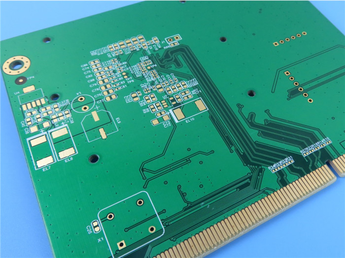
Multi-layer Printed Circuit Board (PCB) HDI Low Loss High Temperature PCB With 90
Ohm Impedance Controlled
(Printed
Circuit Boards are custom-made products, the picture and parameters shown are
just for reference)
Brief
Introduction
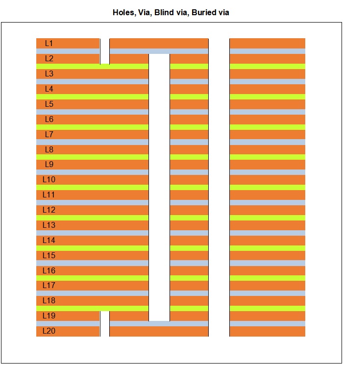
It’s also a type of HDI circuit
boards (N+1+N) with 0.1mm laser drill. This is also a type of impedance
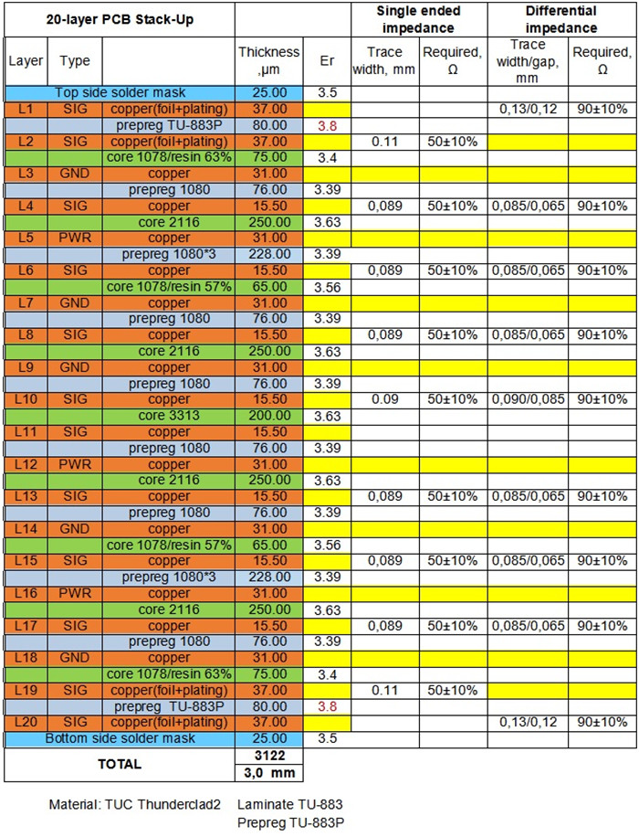
controlled PCB, 90 Ohms and 50 Ohms are controlled on each signal layers with
10% tolerance. The copper foils are 1 oz and half oz used alternately between
layers. The whole PCB is 3.0mm thick, with immersion gold on pads, green solder
mask and white silkscreen.
Applications
Radio
frequency
Backplane,
High performance computing
Line
cards, Storage
Servers,
Telecom, Base station, Office Routers

Detailed
Specifications
|
Item
|
Description
|
Actual
|
Result
|
|
1. Laminate
|
Material Type
|
TU-883
|
ACC
|
|
Tg
|
170℃
|
ACC
|
|
Supplier
|
TUC
|
ACC
|
|
Thickness
|
2.8-3.1mm
|
ACC
|
|
2.Plating thickness
|
Hole Wall
|
26.51µm
|
ACC
|
|
Outer copper
|
41.09µm
|
ACC
|
|
Inner Copper
|
15µm / 31µm
|
ACC
|
|
3.Solder mask
|
Material Type
|
TAIYO/ PSR-2000GT600D
|
ACC
|
|
Color
|
Green
|
ACC
|
|
Rigidity (Pencil Test)
|
5H
|
ACC
|
|
S/M Thickness
|
20.11µm
|
ACC
|
|
Location
|
Both Sides
|
ACC
|
|
4. Component
Mark
|
Material Type
|
IJR-4000 MW300
|
ACC
|
|
Color
|
White
|
ACC
|
|
Location
|
C/S, S/S
|
ACC
|
|
5. Peelable Solder Mask
|
Material Type
|
/
|
|
|
Thickness
|
/
|
|
|
Location
|
/
|
|
|
6. Identification
|
UL Mark
|
YES
|
ACC
|
|
Date Code
|
2921
|
ACC
|
|
Mark Location
|
Solder Side
|
ACC
|
|
7. Surface Finish
|
Method
|
Immersion Gold
|
ACC
|
|
Nickel Thickness
|
4.06µm
|
ACC
|
|
Gold Thickness
|
0.056µm
|
ACC
|
|
8. Normativeness
|
RoHS
|
Directive 2015/863/EU
|
ACC
|
|
REACH
|
Directive 1907 /2006
|
ACC
|
|
9.Annular Ring
|
Min. Line Width (mil)
|
4.8mil
|
ACC
|
|
Min. Spacing (mil)
|
5.2mil
|
ACC
|
|
10.V-groove
|
Angle
|
/
|
|
|
Residual thickness
|
/
|
|
|
11. Beveling
|
Angle
|
/
|
|
|
Height
|
/
|
|
|
12. Function
|
Electrical Test
|
100% PASS
|
ACC
|
|
13. Appearance
|
IPC Class Level
|
IPC-A-600J &6012D
Class 2
|
ACC
|
|
Visual Inspection
|
IPC-A-600J &6012D Class 2
|
ACC
|
|
Warp and Twist
|
0.21%
|
ACC
|
|
14. Reliability Test
|
Tape Test
|
No Peeling
|
ACC
|
|
Solvent Test
|
No Peeling
|
ACC
|
|
Solderability Test
|
265 ±5℃
|
ACC
|
|
Thermal Stress Test
|
288 ±5℃
|
ACC
|
|
Ionic Contamination Test
|
0.56µg/c㎡
|
ACC
|
Stackup
& Impedance Controlled

HDI
vias

MANUFACTURING PROCESS:

BICHENG PCB WORKSHOP:
BICHENG PCB CERTIFICATE:
BICHENG MAIN COURIERS:
